Kyoto Semiconductor kondigt een fotodiode aan in de kleinste klasse van de branche, met een breed scala aan gevoeligheidsgolflengten, van 400 tot 1.700 nm
Ontwikkeling van de KP-2 tweekleurige fotodiode KPMC29, een opbouwmodel voor het meten van licht in twee golflengten langs dezelfde lichtas
TOKIO– (BUSINESS WIRE) – In de veertig jaar sinds de oprichting van het bedrijf heeft Kyoto Semiconductor Co., Ltd., Tsuneo Takahashi, president en CEO, met hoofdkantoor in de wijk Fushimi, Kyoto, de sector geleid met optische oplossingen die zijn gebouwd vanuit technologieën van wereldklasse en met Japanse kwaliteit en aandacht voor productiedetail. Ze hebben de ontwikkeling aangekondigd van een tweegolflengte-fotodiode, de KP-2-tweekleurige fotodiode KPMC29, in de kleinste klasse in de branche en geschikt voor opbouwmontage, met fotodioden van silicium en indium-gallium-arsenide, met lichtgevoeligheid voor een breed golflengtebereik, van 400 tot 1.700 nm, gerangschikt langs dezelfde lichtas.
Dit persbericht bevat multimedia. Bekijk hier de volledige release: https://www.businesswire.com/news/home/20200525005017/en/
Kyoto Semiconductor Announces a Photodiode in the Industry’s Smallest Class, with a Broad Range of Sensitivity Wavelengths, from 400 to 1,700 nm
Developing the KP-2 Two-tone Photodiode KPMC29, a Surface-Mounted Model for Measuring Light in Two Wavelengths Along the Same Light Axis
TOKYO–(BUSINESS WIRE)– In the forty years since the company’s founding, Kyoto Semiconductor Co., Ltd., Tsuneo Takahashi, President and CEO, and headquartered in Fushimi Ward, Kyoto, has led the industry with optical solutions built from world-standard technologies and with Japanese quality and attention to production detail. They have announced the development of a Two-Wavelength Photodiode, the KP-2 Two-tone Photodiode KPMC29, in the industry’s smallest class and capable of being surface-mounted, with silicon and indium-gallium-arsenide photodiodes, with photosensitivity for a wide range of wavelengths, from 400 to 1,700 nm, arrayed along the same light axis.
This press release features multimedia. View the full release here: https://www.businesswire.com/news/home/20200525005017/en/

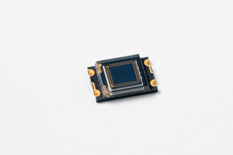
Kyoto Semiconductor KP-2 Two-tone Photodiode KPMC29 (Photo: Business Wire)
This broadband sensitivity, together with a smaller package that is 1/8 the volume ratio of older Kyoto Semiconductor products, can be used in the healthcare field for applications that include medical biometric monitoring like pulse oximeters as well as wearable activity monitors. Because it is also possible to independently produce photocurrent signals from the silicon and indium-gallium-arsenide photodiodes, measuring the photocurrent ratio will allow for its use as a radiation thermometer that can measure temperatures without direct contact with hot object.
Development Background
Spectroscopic analysis technology, that allows for the identification of objects and their characteristics without needing direct contact with those objects, by reflecting light of those objects and measuring the degrees of transmission and reflection, is increasingly needed in a wide range of fields, including medicine, production, and security. Spectroscopic analysis relies on two factors for successful use in identifying a wide range of objects: a wider range of wavelengths, or colors, for the source wavelengths, and a wider range of sensitivity for those wavelengths with the photodiode end. There is also a need for smaller products, compared to existing corded-lead products, for use with medical equipment or wearable devices that can be worn directly on the human body.
Development was therefore undertaken to meet these product needs.
Product Characteristics
- A wider range of wavelength sensitivity (400~1,700nm).
To expand the wavelength range, we layered both silicon photodiodes, which are sensitive to shorter wavelengths, and indium-gallium-arsenide photodiodes, which are sensitive to longer wavelengths, along the same light axis.
- A compact surface-mountable package in the industry’s smallest class.
To successfully make this KP-2 two-tone PD smaller, the indium-gallium-arsenide photodiodes were laid down in pits arranged on the base for the silicon photodiodes, which ordinarily allows light to pass through. This allowed for the package height to be as low as possible. (Patents have been filed.)
Compared to earlier products from Kyoto Semiconductor, the volume ratio has been reduced to 1/8.
See the following for more information. (https://www.kyosemi.co.jp/en/lp/kpmc29/)
Samples will be available from August 31, 2020.
Mass production orders will begin on April 1, 2021.
Kyoto Semiconductor
Kyoto Semiconductor was established in 1980 in Kyoto as a dedicated manufacturer of optical semiconductors. The semiconductors manufactured offer superlative performance and precision, suited for use in optical transmission. They are manufactured end-to-end, including pre- and post-processing, and together with Kyoto Semiconductor’s unique packaging technology, at our location in Japan and made available to customers around the world. Kyoto Semiconductor leads the industry with world-standard technologies for optical device solutions based on Japanese quality and attention to production detail.
Company Website: https://www.kyosemi.co.jp/
View source version on businesswire.com: https://www.businesswire.com/news/home/20200525005017/en/
Contacts
Direct inquiries to:
Media Relations, Kyoto Semiconductor Co., Ltd.
Naoko Kodama
Email: Media_relation@kyosemi.co.jp

