Heptagon ontwikkelt ‘s werelds kleinste optische sensormodule voor nabije veld
SANTA CLARA, Calif.–(BUSINESS WIRE)– Heptagon ( www.hptg.com) heeft vandaag bekendgemaakt dat het ‘s werelds kleinste module voor optische waarneming in het nabije veld heeft ontwikkeld. Het bedrijf baseerde de module op zijn hypermoderne miniaturisatietechnologie van waferklasse. De nieuwe sensor heeft een dikte van 350 micron en een oppervlakte van 2 vierkante millimeter. Het bestaat uit een ingebouwde verlichter, een lichtsensor, elektronica, functies ter voorkoming van overspraak en een lenssysteem. Dit is de technologische basis van Heptagons nieuwe generatie sterk geminiaturiseerde System-in-a-package-sensoren voor markten die zich snel ontwikkelen, zoals die voor mobiele apparatuur en wearables. De moderne, optisch-elektrische productietechnologie voor de creatie van deze piepkleine sensormodule onderstreept de wereldklasse van het bedrijf op gebied van onderzoek en ontwikkeling. Bovendien benadrukt het Heptagons expertise in miniaturisatietechnologie op waferniveau, waaronder optica, stacking en integratie op waferniveau. Het bedrijf is klaar voor massale productie en gebruikt Wafer Level Process (WLP)-technologie voor hoge kwaliteit, productiviteit en consistentie.
Heptagon Develops World’s Smallest Near-Field Optical Sensing Module Based on Company’s Patented State-of-the-Art Wafer-Level Miniaturization Technology
SANTA CLARA, Calif.–(BUSINESS WIRE)– Heptagon ( www.hptg.com), today announced it has developed the world’s smallest near-field optical sensing module based on the company’s state-of-the-art wafer-level miniaturization technology. The new sensor has a thickness of only 350 microns and a 2mm 2 surface area, which includes a built-in illuminator, light sensor, electronics, crosstalk prevention features, and a lens system. This demonstrates the technology foundation for Heptagon’s next generation of highly-miniaturized System-in-a-Package sensors in rapidly evolving markets such as mobile and wearable devices. The state-of-the-art manufacturing and optical-electrical technology used to create this tiny new sensor module, underscores the company’s world-class R&D and highlights Heptagon’s expertise in wafer-level miniaturization technology, including wafer-level optics, stacking, and integration. It is mass production ready and uses Wafer Level Process (WLP) technology to achieve high yield, quality and consistency.
This Smart News Release features multimedia. View the full release here: http://www.businesswire.com/news/home/20160221005207/en/
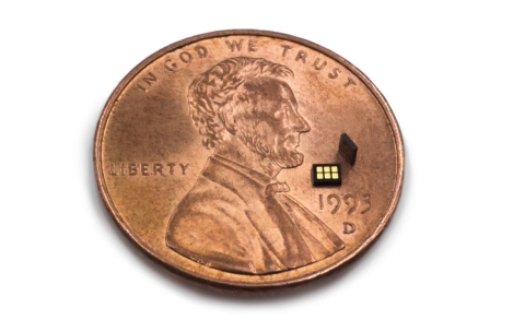
 Heptagon’s new module is 4x thinner than a penny – US 1 cent coin (Photo: Business Wire)
“We are excited to be taking our sensor technologies to an all new level,” says Hartmut Rudmann, Senior VP of Engineering at Heptagon, “By combining proprietary design and processes in solution development for these significantly thinner sensors, we’re enabling greater design flexibility with reduced form factor and improved aesthetics for mobile and wearable devices seeking slimmer profiles, such as smart watches. It is now possible to spread out more sensors in a device to increase coverage or for a more accurate reading.”
Heptagon’s wafer-level process technology enables it to manufacture high volumes of highly accurate, advanced opto-electronic products onto a single wafer with very high yields. The benefits of this process technology include economies of scale, fast ramp to high production volumes, high levels of integration and miniaturization, and precise location of micro-structures. The company has developed proprietary, patented wafer-level manufacturing processes in three areas, wafer-level optics used to create nanometer optical structures, wafer-level stacking for reflowable pads, and wafer-level integration for stacked optics and filters.
The new complete sensor module is only 350 microns thick, which includes electronics, a sensor and illuminator, packaging and a lens system. To put that into perspective, Heptagon’s new module is 4x thinner than a US 1 cent coin. Comparable products currently available are 40% thicker. With its ultra-thin profile, this new technology is ideally suited for integrating contact-sensing and skin-proximity detection functionality in next generation wearable devices, smartphones and ultra-thin notebooks. Additional applications are invisible buttons for use in sealed or improved esthetics products, vital signs monitoring in healthcare, intelligence door handles or car gear shifts.
Heptagon’s highly experienced engineering teams have specialized in high-volume design and manufacture of miniaturized technologies for over 20 years. The capability to integrate heterogeneous technologies in miniaturized packages is rapidly becoming the enabler of next generation products in mobile, wearables and IoT. Introducing the world’s smallest proximity sensor is another example of Heptagon’s innovation and world class optical-electrical R&D.
About Heptagon
Heptagon ( www.hptg.com) provides complete 3D/imaging, illumination and optical sensing solutions for smart devices and the internet of things. With over 2 billion units shipped and 20 years of industry firsts in miniaturizing and integrating complex hardware and software systems, Heptagon has industry leading technology and services to enhance our customer’s competitiveness. Backed by world-class investors, Heptagon is a global company with research and development, sales and customer services teams located in Singapore, Zurich Switzerland, in Silicon Valley USA, and Shenzhen China.
View source version on businesswire.com: http://www.businesswire.com/news/home/20160221005207/en/
Contacts
Heptagon
Scott Filler, +1 408-329-8920
pr@hptg.com
